EE559 – Integrated Analog Electronic Circuits
Mini Project
Electronics laboratory
OBJECTIVE:
- To become familiarize with designing a long tail pair for given parameters.
- To implement the hardware setup for long tail pair.
- To observe the characteristics of the implemented long tail pair.
-Maximum undistorted output swing.
-DC voltage gain.
-Common mode rejection ratio.
-3dB bandwidth.
APPARATUS:
- SSM2212 SMD dual transistors (2 ICs)
- 680 Ohm 1206 SMD resistors
- 1.8 kOhm 1206 SMD resistors
- 6.8 kOhm 1206 SMD resistors
CIRCUIT DIAGRAM:
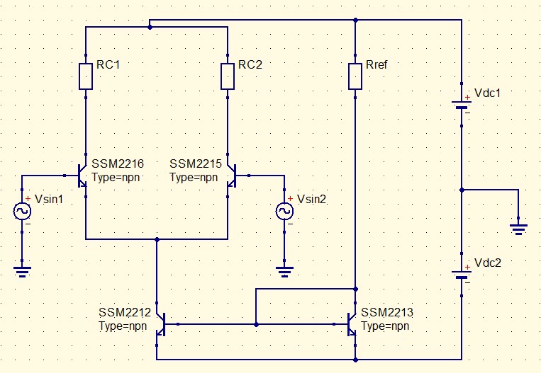
Figure1. Schematic diagram of the long tail pair
THEORY:
Using KVL ……….. (1)
Using KCL ……….. (2)
Trans-conductance ……….. (3)
DC Voltage gain ……….. (4)
Maximum Undistorted
Output swing ……….. (5)
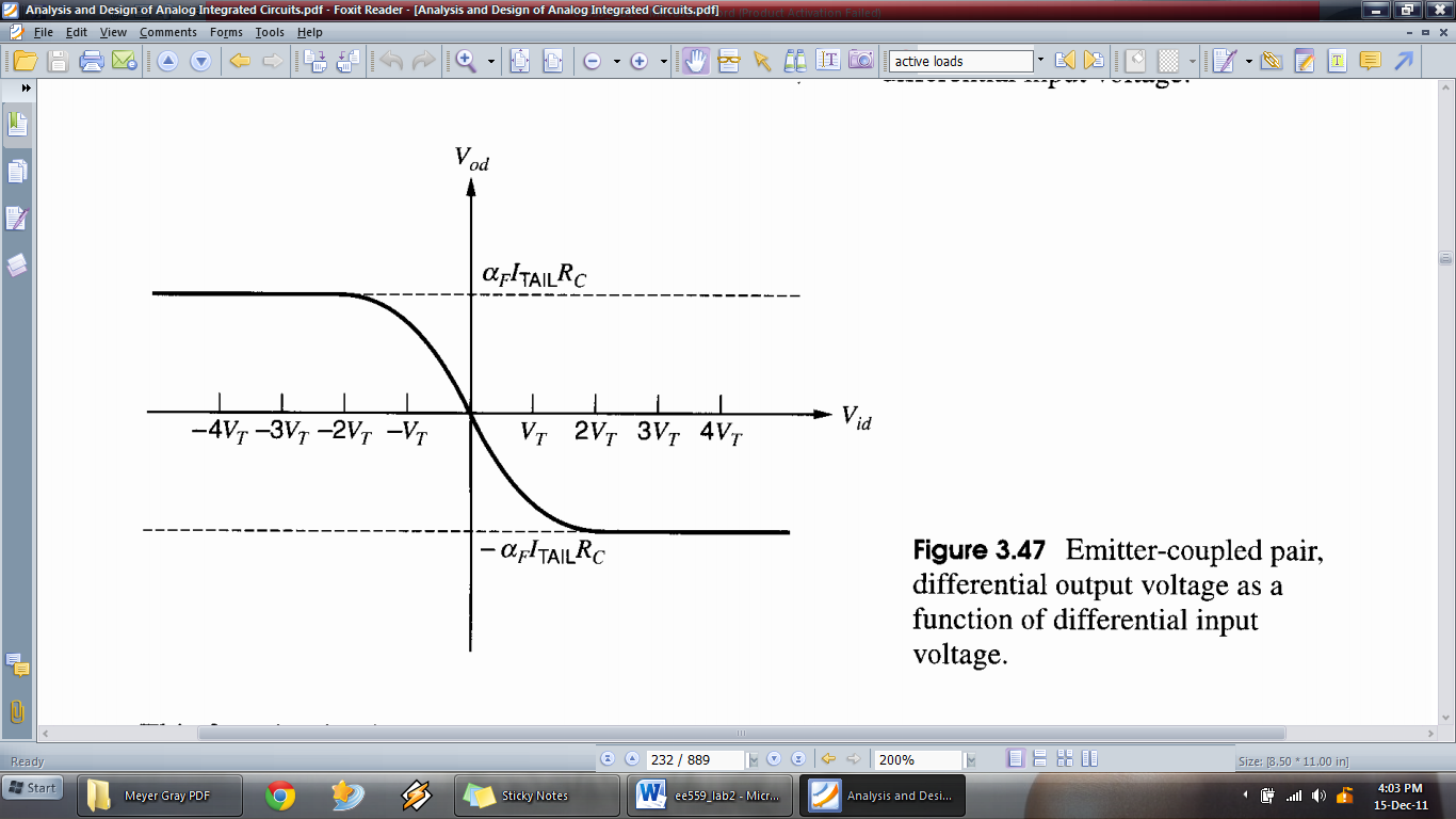
Figure 2. Relevant Graphs and Equations
PROCEDURE:
- Select and calculate Vdc1, Vdc2, Rref and Rc values for the given specifications.
- DC voltage gain (AV) : 10 ( 20log(AV) = 20 dB )
- Maximum undistorted output swing : 1V
- Simulate above circuit using QUCS software and observe following parameters.
- Maximum undistorted output swing.
- DC voltage gain
- Input and output waveforms for 200 Hz
- Differential gain for 0 to 100MHz
- Common mode gain for 0 to 100MHz
- CMRR for 0 to 100MHz
- 3dB bandwidth
- Use a PCB layout designing software (eg. PROTEUS) to design the PCB layout.
(Note: You should show this design to instructor before implementing hardware)
- Using selected resistor values and transistor ICs implement the hardware.
- Take following observations to verify the operation of the long tail pair.
- Observe output differential voltage by applying -200mV to 200mv input differential DC voltage in the steps of 10mV and plot input differential voltage vs. output differential voltage in order to observe maximum undistorted output voltage swing.
- From the above graph identify DC voltage gain.
- Apply 10mV differential DC input voltage and observe the amplification.
- Apply 200Hz 10mV sinusoidal differential input and observe the output differential waveform.
- For differential mode change the frequency of the input differential sinusoidal and observe output waveform for 0, 10Hz, 100Hz, 1 kHz, 10 kHz, 100 kHz, 1 MHz, 10 MHz, and 100 MHz and plot frequency (dB) vs. Differential mode gain plot.
- For common mode change the frequency and observe output waveform for 0, 10Hz, 100Hz, 1 kHz, 10 kHz, 100 kHz, 1 MHz, 10 MHz, and 100 MHz and plot frequency (dB) vs. Common mode gain plot.
- Using above values obtain the frequency (dB) vs. CMRR plot.
- Using the results obtain the 3dB bandwidth of the differential amplifier.

7 comments